- 您现在的位置:买卖IC网 > Sheet目录488 > NTF3055-100T3LF (ON Semiconductor)MOSFET N-CH 60V 3A SOT223
�� �
�
�NTF3055-100,�
�NVF3055-100�
�Power� MOSFET�
�3.0� Amps,� 60� Volts�
�N� ?� Channel� SOT� ?� 223�
�Designed� for� low� voltage,� high� speed� switching� applications� in�
�power� supplies,� converters� and� power� motor� controls� and� bridge�
�circuits.�
�Features�
�?� AEC� ?� Q101� Qualified� and� PPAP� Capable� ?� NVF3055� ?� 100�
�?� These� Devices� are� Pb� ?� Free� and� are� RoHS� Compliant�
�http://onsemi.com�
�3.0� A,� 60� V�
�R� DS(on)� =� 110� m� W�
�N� ?� Channel�
�D�
�Applications�
�?� Power� Supplies�
�?� Converters�
�?� Power� Motor� Controls�
�?� Bridge� Circuits�
�MAXIMUM� RATINGS� (T� C� =� 25� °� C� unless� otherwise� noted)�
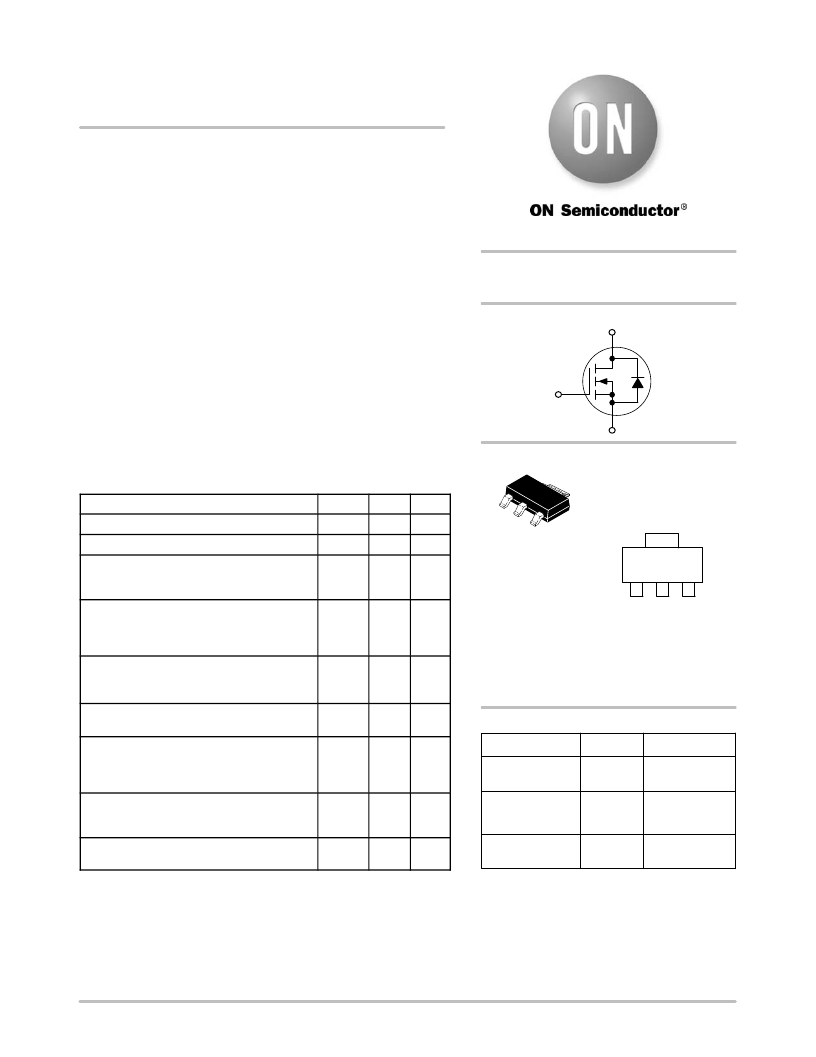
�G�
�4�
�S�
�MARKING�
�DIAGRAM�
�&� PIN�
�Rating�
�Drain� ?� to� ?� Source� Voltage�
�Drain� ?� to� ?� Gate� Voltage� (R� GS� =� 10� M� W� )�
�Gate� ?� to� ?� Source� Voltage�
�?� Continuous�
�?� Non� ?� repetitive� (t� p� ≤� 10� ms)�
�Symbol�
�V� DSS�
�V� DGR�
�V� GS�
�Value�
�60�
�60�
�±� 20�
�±� 30�
�Unit�
�Vdc�
�Vdc�
�Vdc�
�Vpk�
�1�
�2�
�3�
�SOT� ?� 223�
�CASE� 318E�
�STYLE� 3�
�ASSIGNMENT�
�Drain�
�4�
�AWW�
�3055� G�
�G�
�Drain� Current�
�?� Continuous� @� T� A� =� 25� °� C�
�?� Continuous� @� T� A� =� 100� °� C�
�?� Single� Pulse� (t� p� ≤� 10� m� s)�
�Total� Power� Dissipation� @� T� A� =� 25� °� C� (Note� 1)�
�Total� Power� Dissipation� @� T� A� =� 25� °� C� (Note� 2)�
�Derate� above� 25� °� C�
�Operating� and� Storage� Temperature� Range�
�I� D�
�I� D�
�I� DM�
�P� D�
�T� J� ,� T� stg�
�3.0�
�1.4�
�9.0�
�2.1�
�1.3�
�0.014�
�?� 55�
�to� 175�
�Adc�
�Apk�
�W�
�W�
�W/� °� C�
�°� C�
�1� 2� 3�
�Gate� Drain� Source�
�A� =� Assembly� Location�
�WW� =� Work� Week�
�3055� =� Specific� Device� Code�
�G� =� Pb� ?� Free� Package�
�(Note:� Microdot� may� be� in� either� location)�
�ORDERING� INFORMATION�
�Single� Pulse� Drain� ?� to� ?� Source� Avalanche�
�Energy� ?� Starting� T� J� =� 25� °� C�
�(V� DD� =� 25� Vdc,� V� GS� =� 10� Vdc,�
�I� L� (pk)� =� 7.0� Apk,� L� =� 3.0� mH,� V� DS� =� 60� Vdc)�
�Thermal� Resistance�
�?� Junction� ?� to� ?� Ambient� (Note� 1)�
�?� Junction� ?� to� ?� Ambient� (Note� 2)�
�Maximum� Lead� Temperature� for� Soldering�
�Purposes,� 1/8� ″� from� case� for� 10� seconds�
�E� AS�
�R� q� JA�
�R� q� JA�
�T� L�
�74�
�72.3�
�114�
�260�
�mJ�
�°� C/W�
�°� C�
�Device�
�NTF3055� ?� 100T1G�
�NTF3055� ?� 100T3G�
�NVF3055� ?� 100T1G�
�Package�
�SOT� ?� 223�
�(Pb� ?� Free)�
�SOT� ?� 223�
�(Pb� ?� Free)�
�SOT� ?� 223�
�(Pb� ?� Free)�
�Shipping� ?�
�1000� /� Tape� &�
�Reel�
�4000� /� Tape� &�
�Reel�
�1000� /� Tape� &�
�Reel�
�Stresses� exceeding� Maximum� Ratings� may� damage� the� device.� Maximum�
�Ratings� are� stress� ratings� only.� Functional� operation� above� the� Recommended�
�Operating� Conditions� is� not� implied.� Extended� exposure� to� stresses� above� the�
�Recommended� Operating� Conditions� may� affect� device� reliability.�
�1.� When� surface� mounted� to� an� FR4� board� using� 1� ″� pad� size,� 1� oz.�
�(Cu.� Area� 1.127� sq� in).�
�2.� When� surface� mounted� to� an� FR4� board� using� minimum� recommended� pad�
�size,� 2� ?� 2.4� oz.� (Cu.� Area� 0.272� sq� in).�
�?For� information� on� tape� and� reel� specifications,�
�including� part� orientation� and� tape� sizes,� please�
�refer� to� our� Tape� and� Reel� Packaging� Specifications�
�Brochure,� BRD8011/D.�
�?� Semiconductor� Components� Industries,� LLC,� 2011�
�October,� 2011� ?� Rev.� 4�
�1�
�Publication� Order� Number:�
�NTF3055� ?� 100/D�
�发布紧急采购,3分钟左右您将得到回复。
相关PDF资料
NTF3055-160T1
MOSFET N-CH 60V 2A SOT223
NTF3055L108T3LFG
MOSFET N-CH 60V 3A SOT223
NTF3055L175T1
MOSFET N-CH 60V 2A SOT223
NTF5P03T3G
MOSFET P-CH 30V 3.7A SOT223
NTF6P02T3G
MOSFET PWR P-CHAN 10A 20V SOT223
NTGD3133PT1G
MOSFET P-CH DUAL 20V 21.5A 6TSOP
NTGD3147FT1G
MOSFET P-CH 20V 2.2A 6-TSOP
NTGD3148NT1G
MOSFET N-CH DUAL 20V 3.5A 6TSOP
相关代理商/技术参数
NTF3055-160
制造商:ONSEMI 制造商全称:ON Semiconductor 功能描述:Power MOSFET 2.0 Amps, 60 Volts N-Channel SOT-223
NTF3055-160T1
功能描述:MOSFET N-CH 60V 2A SOT223 RoHS:否 类别:分离式半导体产品 >> FET - 单 系列:- 标准包装:1,000 系列:MESH OVERLAY™ FET 型:MOSFET N 通道,金属氧化物 FET 特点:逻辑电平门 漏极至源极电压(Vdss):200V 电流 - 连续漏极(Id) @ 25° C:18A 开态Rds(最大)@ Id, Vgs @ 25° C:180 毫欧 @ 9A,10V Id 时的 Vgs(th)(最大):4V @ 250µA 闸电荷(Qg) @ Vgs:72nC @ 10V 输入电容 (Ciss) @ Vds:1560pF @ 25V 功率 - 最大:40W 安装类型:通孔 封装/外壳:TO-220-3 整包 供应商设备封装:TO-220FP 包装:管件
NTF3055-160T3
制造商:Rochester Electronics LLC 功能描述:- Bulk
NTF3055-160T3LF
功能描述:MOSFET N-CH 60V 2A SOT223 RoHS:否 类别:分离式半导体产品 >> FET - 单 系列:- 标准包装:1,000 系列:MESH OVERLAY™ FET 型:MOSFET N 通道,金属氧化物 FET 特点:逻辑电平门 漏极至源极电压(Vdss):200V 电流 - 连续漏极(Id) @ 25° C:18A 开态Rds(最大)@ Id, Vgs @ 25° C:180 毫欧 @ 9A,10V Id 时的 Vgs(th)(最大):4V @ 250µA 闸电荷(Qg) @ Vgs:72nC @ 10V 输入电容 (Ciss) @ Vds:1560pF @ 25V 功率 - 最大:40W 安装类型:通孔 封装/外壳:TO-220-3 整包 供应商设备封装:TO-220FP 包装:管件
NTF3055L108
制造商:ONSEMI 制造商全称:ON Semiconductor 功能描述:Power MOSFET 3.0 A, 60 V, Logic Level, N−Channel SOT−223
NTF3055L108/D
制造商:未知厂家 制造商全称:未知厂家 功能描述:Power MOSFET 3.0 Amps, 60 Volts, Logic Level
NTF3055L108D
制造商:ONSEMI 制造商全称:ON Semiconductor 功能描述:Power MOSFET 3.0 A, 60 V, Logic Level, N−Channel SOT−223
NTF3055L108T1
功能描述:MOSFET 60V 3A N-Channel RoHS:否 制造商:STMicroelectronics 晶体管极性:N-Channel 汲极/源极击穿电压:650 V 闸/源击穿电压:25 V 漏极连续电流:130 A 电阻汲极/源极 RDS(导通):0.014 Ohms 配置:Single 最大工作温度: 安装风格:Through Hole 封装 / 箱体:Max247 封装:Tube